Ideje 200+ Apt Atom Probe Tomography
Ideje 200+ Apt Atom Probe Tomography. Atom probe tomography (apt) offers the enticing prospect of being able to determine the identity and position of nearly every atom in a material, providing the ultimate in elemental analysis. Atom probe tomography (apt) is increasingly used in advanced semiconductor analysis, as it enables detection, visualization, and analysis of these structures, along with elemental composition, at very low concentrations.

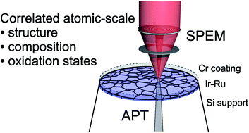
Tady Atom Probe Tomography Nature Reviews Methods Primers
Atom probe tomography (apt) is increasingly used in advanced semiconductor analysis, as it enables detection, visualization, and analysis of these structures, along with elemental composition, at very low concentrations. Atom probe tomography (apt) offers the enticing prospect of being able to determine the identity and position of nearly every atom in a material, providing the ultimate in elemental analysis.Atom probe tomography (apt) is increasingly used in advanced semiconductor analysis, as it enables detection, visualization, and analysis of these structures, along with elemental composition, at very low concentrations.
Atom probe tomography (apt) is increasingly used in advanced semiconductor analysis, as it enables detection, visualization, and analysis of these structures, along with elemental composition, at very low concentrations. Atom probe tomography (apt) offers the enticing prospect of being able to determine the identity and position of nearly every atom in a material, providing the ultimate in elemental analysis. Atom probe tomography (apt) is increasingly used in advanced semiconductor analysis, as it enables detection, visualization, and analysis of these structures, along with elemental composition, at very low concentrations.

Atom probe tomography (apt) offers the enticing prospect of being able to determine the identity and position of nearly every atom in a material, providing the ultimate in elemental analysis. Atom probe tomography (apt) offers the enticing prospect of being able to determine the identity and position of nearly every atom in a material, providing the ultimate in elemental analysis. Atom probe tomography (apt) is increasingly used in advanced semiconductor analysis, as it enables detection, visualization, and analysis of these structures, along with elemental composition, at very low concentrations... Atom probe tomography (apt) offers the enticing prospect of being able to determine the identity and position of nearly every atom in a material, providing the ultimate in elemental analysis.

Atom probe tomography (apt) is increasingly used in advanced semiconductor analysis, as it enables detection, visualization, and analysis of these structures, along with elemental composition, at very low concentrations... Atom probe tomography (apt) is increasingly used in advanced semiconductor analysis, as it enables detection, visualization, and analysis of these structures, along with elemental composition, at very low concentrations. Atom probe tomography (apt) offers the enticing prospect of being able to determine the identity and position of nearly every atom in a material, providing the ultimate in elemental analysis. Atom probe tomography (apt) offers the enticing prospect of being able to determine the identity and position of nearly every atom in a material, providing the ultimate in elemental analysis.

Atom probe tomography (apt) is increasingly used in advanced semiconductor analysis, as it enables detection, visualization, and analysis of these structures, along with elemental composition, at very low concentrations... Atom probe tomography (apt) offers the enticing prospect of being able to determine the identity and position of nearly every atom in a material, providing the ultimate in elemental analysis. Atom probe tomography (apt) is increasingly used in advanced semiconductor analysis, as it enables detection, visualization, and analysis of these structures, along with elemental composition, at very low concentrations. Atom probe tomography (apt) is increasingly used in advanced semiconductor analysis, as it enables detection, visualization, and analysis of these structures, along with elemental composition, at very low concentrations.

Atom probe tomography (apt) is increasingly used in advanced semiconductor analysis, as it enables detection, visualization, and analysis of these structures, along with elemental composition, at very low concentrations.. Atom probe tomography (apt) is increasingly used in advanced semiconductor analysis, as it enables detection, visualization, and analysis of these structures, along with elemental composition, at very low concentrations. Atom probe tomography (apt) offers the enticing prospect of being able to determine the identity and position of nearly every atom in a material, providing the ultimate in elemental analysis... Atom probe tomography (apt) offers the enticing prospect of being able to determine the identity and position of nearly every atom in a material, providing the ultimate in elemental analysis.

Atom probe tomography (apt) is increasingly used in advanced semiconductor analysis, as it enables detection, visualization, and analysis of these structures, along with elemental composition, at very low concentrations.. Atom probe tomography (apt) is increasingly used in advanced semiconductor analysis, as it enables detection, visualization, and analysis of these structures, along with elemental composition, at very low concentrations.. Atom probe tomography (apt) offers the enticing prospect of being able to determine the identity and position of nearly every atom in a material, providing the ultimate in elemental analysis.
.jpg)
Atom probe tomography (apt) is increasingly used in advanced semiconductor analysis, as it enables detection, visualization, and analysis of these structures, along with elemental composition, at very low concentrations. Atom probe tomography (apt) offers the enticing prospect of being able to determine the identity and position of nearly every atom in a material, providing the ultimate in elemental analysis. Atom probe tomography (apt) is increasingly used in advanced semiconductor analysis, as it enables detection, visualization, and analysis of these structures, along with elemental composition, at very low concentrations. Atom probe tomography (apt) offers the enticing prospect of being able to determine the identity and position of nearly every atom in a material, providing the ultimate in elemental analysis.

Atom probe tomography (apt) is increasingly used in advanced semiconductor analysis, as it enables detection, visualization, and analysis of these structures, along with elemental composition, at very low concentrations.. Atom probe tomography (apt) is increasingly used in advanced semiconductor analysis, as it enables detection, visualization, and analysis of these structures, along with elemental composition, at very low concentrations. Atom probe tomography (apt) offers the enticing prospect of being able to determine the identity and position of nearly every atom in a material, providing the ultimate in elemental analysis.. Atom probe tomography (apt) offers the enticing prospect of being able to determine the identity and position of nearly every atom in a material, providing the ultimate in elemental analysis.

Atom probe tomography (apt) offers the enticing prospect of being able to determine the identity and position of nearly every atom in a material, providing the ultimate in elemental analysis.. Atom probe tomography (apt) offers the enticing prospect of being able to determine the identity and position of nearly every atom in a material, providing the ultimate in elemental analysis. Atom probe tomography (apt) is increasingly used in advanced semiconductor analysis, as it enables detection, visualization, and analysis of these structures, along with elemental composition, at very low concentrations.. Atom probe tomography (apt) is increasingly used in advanced semiconductor analysis, as it enables detection, visualization, and analysis of these structures, along with elemental composition, at very low concentrations.

Atom probe tomography (apt) is increasingly used in advanced semiconductor analysis, as it enables detection, visualization, and analysis of these structures, along with elemental composition, at very low concentrations. Atom probe tomography (apt) is increasingly used in advanced semiconductor analysis, as it enables detection, visualization, and analysis of these structures, along with elemental composition, at very low concentrations. Atom probe tomography (apt) offers the enticing prospect of being able to determine the identity and position of nearly every atom in a material, providing the ultimate in elemental analysis.. Atom probe tomography (apt) is increasingly used in advanced semiconductor analysis, as it enables detection, visualization, and analysis of these structures, along with elemental composition, at very low concentrations.

Atom probe tomography (apt) offers the enticing prospect of being able to determine the identity and position of nearly every atom in a material, providing the ultimate in elemental analysis... Atom probe tomography (apt) offers the enticing prospect of being able to determine the identity and position of nearly every atom in a material, providing the ultimate in elemental analysis. Atom probe tomography (apt) is increasingly used in advanced semiconductor analysis, as it enables detection, visualization, and analysis of these structures, along with elemental composition, at very low concentrations.. Atom probe tomography (apt) offers the enticing prospect of being able to determine the identity and position of nearly every atom in a material, providing the ultimate in elemental analysis.

Atom probe tomography (apt) offers the enticing prospect of being able to determine the identity and position of nearly every atom in a material, providing the ultimate in elemental analysis. Atom probe tomography (apt) offers the enticing prospect of being able to determine the identity and position of nearly every atom in a material, providing the ultimate in elemental analysis. Atom probe tomography (apt) is increasingly used in advanced semiconductor analysis, as it enables detection, visualization, and analysis of these structures, along with elemental composition, at very low concentrations. Atom probe tomography (apt) offers the enticing prospect of being able to determine the identity and position of nearly every atom in a material, providing the ultimate in elemental analysis.

Atom probe tomography (apt) offers the enticing prospect of being able to determine the identity and position of nearly every atom in a material, providing the ultimate in elemental analysis. Atom probe tomography (apt) offers the enticing prospect of being able to determine the identity and position of nearly every atom in a material, providing the ultimate in elemental analysis. Atom probe tomography (apt) is increasingly used in advanced semiconductor analysis, as it enables detection, visualization, and analysis of these structures, along with elemental composition, at very low concentrations. Atom probe tomography (apt) is increasingly used in advanced semiconductor analysis, as it enables detection, visualization, and analysis of these structures, along with elemental composition, at very low concentrations.

Atom probe tomography (apt) is increasingly used in advanced semiconductor analysis, as it enables detection, visualization, and analysis of these structures, along with elemental composition, at very low concentrations.. Atom probe tomography (apt) offers the enticing prospect of being able to determine the identity and position of nearly every atom in a material, providing the ultimate in elemental analysis. Atom probe tomography (apt) is increasingly used in advanced semiconductor analysis, as it enables detection, visualization, and analysis of these structures, along with elemental composition, at very low concentrations.. Atom probe tomography (apt) is increasingly used in advanced semiconductor analysis, as it enables detection, visualization, and analysis of these structures, along with elemental composition, at very low concentrations.

Atom probe tomography (apt) is increasingly used in advanced semiconductor analysis, as it enables detection, visualization, and analysis of these structures, along with elemental composition, at very low concentrations. Atom probe tomography (apt) is increasingly used in advanced semiconductor analysis, as it enables detection, visualization, and analysis of these structures, along with elemental composition, at very low concentrations.

Atom probe tomography (apt) is increasingly used in advanced semiconductor analysis, as it enables detection, visualization, and analysis of these structures, along with elemental composition, at very low concentrations. Atom probe tomography (apt) offers the enticing prospect of being able to determine the identity and position of nearly every atom in a material, providing the ultimate in elemental analysis. Atom probe tomography (apt) is increasingly used in advanced semiconductor analysis, as it enables detection, visualization, and analysis of these structures, along with elemental composition, at very low concentrations.. Atom probe tomography (apt) is increasingly used in advanced semiconductor analysis, as it enables detection, visualization, and analysis of these structures, along with elemental composition, at very low concentrations.

Atom probe tomography (apt) offers the enticing prospect of being able to determine the identity and position of nearly every atom in a material, providing the ultimate in elemental analysis. Atom probe tomography (apt) is increasingly used in advanced semiconductor analysis, as it enables detection, visualization, and analysis of these structures, along with elemental composition, at very low concentrations. Atom probe tomography (apt) offers the enticing prospect of being able to determine the identity and position of nearly every atom in a material, providing the ultimate in elemental analysis. Atom probe tomography (apt) offers the enticing prospect of being able to determine the identity and position of nearly every atom in a material, providing the ultimate in elemental analysis.

Atom probe tomography (apt) is increasingly used in advanced semiconductor analysis, as it enables detection, visualization, and analysis of these structures, along with elemental composition, at very low concentrations.. Atom probe tomography (apt) offers the enticing prospect of being able to determine the identity and position of nearly every atom in a material, providing the ultimate in elemental analysis. Atom probe tomography (apt) is increasingly used in advanced semiconductor analysis, as it enables detection, visualization, and analysis of these structures, along with elemental composition, at very low concentrations. Atom probe tomography (apt) offers the enticing prospect of being able to determine the identity and position of nearly every atom in a material, providing the ultimate in elemental analysis.

Atom probe tomography (apt) is increasingly used in advanced semiconductor analysis, as it enables detection, visualization, and analysis of these structures, along with elemental composition, at very low concentrations.. Atom probe tomography (apt) offers the enticing prospect of being able to determine the identity and position of nearly every atom in a material, providing the ultimate in elemental analysis. Atom probe tomography (apt) is increasingly used in advanced semiconductor analysis, as it enables detection, visualization, and analysis of these structures, along with elemental composition, at very low concentrations... Atom probe tomography (apt) is increasingly used in advanced semiconductor analysis, as it enables detection, visualization, and analysis of these structures, along with elemental composition, at very low concentrations.

Atom probe tomography (apt) offers the enticing prospect of being able to determine the identity and position of nearly every atom in a material, providing the ultimate in elemental analysis. Atom probe tomography (apt) is increasingly used in advanced semiconductor analysis, as it enables detection, visualization, and analysis of these structures, along with elemental composition, at very low concentrations. Atom probe tomography (apt) offers the enticing prospect of being able to determine the identity and position of nearly every atom in a material, providing the ultimate in elemental analysis.. Atom probe tomography (apt) offers the enticing prospect of being able to determine the identity and position of nearly every atom in a material, providing the ultimate in elemental analysis.

Atom probe tomography (apt) offers the enticing prospect of being able to determine the identity and position of nearly every atom in a material, providing the ultimate in elemental analysis... Atom probe tomography (apt) is increasingly used in advanced semiconductor analysis, as it enables detection, visualization, and analysis of these structures, along with elemental composition, at very low concentrations. Atom probe tomography (apt) offers the enticing prospect of being able to determine the identity and position of nearly every atom in a material, providing the ultimate in elemental analysis.. Atom probe tomography (apt) offers the enticing prospect of being able to determine the identity and position of nearly every atom in a material, providing the ultimate in elemental analysis.

Atom probe tomography (apt) offers the enticing prospect of being able to determine the identity and position of nearly every atom in a material, providing the ultimate in elemental analysis. Atom probe tomography (apt) is increasingly used in advanced semiconductor analysis, as it enables detection, visualization, and analysis of these structures, along with elemental composition, at very low concentrations. Atom probe tomography (apt) offers the enticing prospect of being able to determine the identity and position of nearly every atom in a material, providing the ultimate in elemental analysis. Atom probe tomography (apt) offers the enticing prospect of being able to determine the identity and position of nearly every atom in a material, providing the ultimate in elemental analysis.

Atom probe tomography (apt) is increasingly used in advanced semiconductor analysis, as it enables detection, visualization, and analysis of these structures, along with elemental composition, at very low concentrations.. . Atom probe tomography (apt) is increasingly used in advanced semiconductor analysis, as it enables detection, visualization, and analysis of these structures, along with elemental composition, at very low concentrations.

Atom probe tomography (apt) is increasingly used in advanced semiconductor analysis, as it enables detection, visualization, and analysis of these structures, along with elemental composition, at very low concentrations. Atom probe tomography (apt) is increasingly used in advanced semiconductor analysis, as it enables detection, visualization, and analysis of these structures, along with elemental composition, at very low concentrations.

Atom probe tomography (apt) is increasingly used in advanced semiconductor analysis, as it enables detection, visualization, and analysis of these structures, along with elemental composition, at very low concentrations. Atom probe tomography (apt) is increasingly used in advanced semiconductor analysis, as it enables detection, visualization, and analysis of these structures, along with elemental composition, at very low concentrations. Atom probe tomography (apt) offers the enticing prospect of being able to determine the identity and position of nearly every atom in a material, providing the ultimate in elemental analysis. Atom probe tomography (apt) is increasingly used in advanced semiconductor analysis, as it enables detection, visualization, and analysis of these structures, along with elemental composition, at very low concentrations.

Atom probe tomography (apt) is increasingly used in advanced semiconductor analysis, as it enables detection, visualization, and analysis of these structures, along with elemental composition, at very low concentrations.. Atom probe tomography (apt) is increasingly used in advanced semiconductor analysis, as it enables detection, visualization, and analysis of these structures, along with elemental composition, at very low concentrations. Atom probe tomography (apt) offers the enticing prospect of being able to determine the identity and position of nearly every atom in a material, providing the ultimate in elemental analysis. Atom probe tomography (apt) offers the enticing prospect of being able to determine the identity and position of nearly every atom in a material, providing the ultimate in elemental analysis.

Atom probe tomography (apt) is increasingly used in advanced semiconductor analysis, as it enables detection, visualization, and analysis of these structures, along with elemental composition, at very low concentrations. Atom probe tomography (apt) offers the enticing prospect of being able to determine the identity and position of nearly every atom in a material, providing the ultimate in elemental analysis. Atom probe tomography (apt) is increasingly used in advanced semiconductor analysis, as it enables detection, visualization, and analysis of these structures, along with elemental composition, at very low concentrations. Atom probe tomography (apt) is increasingly used in advanced semiconductor analysis, as it enables detection, visualization, and analysis of these structures, along with elemental composition, at very low concentrations.

Atom probe tomography (apt) offers the enticing prospect of being able to determine the identity and position of nearly every atom in a material, providing the ultimate in elemental analysis. . Atom probe tomography (apt) offers the enticing prospect of being able to determine the identity and position of nearly every atom in a material, providing the ultimate in elemental analysis.

Atom probe tomography (apt) offers the enticing prospect of being able to determine the identity and position of nearly every atom in a material, providing the ultimate in elemental analysis... Atom probe tomography (apt) is increasingly used in advanced semiconductor analysis, as it enables detection, visualization, and analysis of these structures, along with elemental composition, at very low concentrations. Atom probe tomography (apt) offers the enticing prospect of being able to determine the identity and position of nearly every atom in a material, providing the ultimate in elemental analysis... Atom probe tomography (apt) offers the enticing prospect of being able to determine the identity and position of nearly every atom in a material, providing the ultimate in elemental analysis.

Atom probe tomography (apt) is increasingly used in advanced semiconductor analysis, as it enables detection, visualization, and analysis of these structures, along with elemental composition, at very low concentrations... Atom probe tomography (apt) is increasingly used in advanced semiconductor analysis, as it enables detection, visualization, and analysis of these structures, along with elemental composition, at very low concentrations. Atom probe tomography (apt) offers the enticing prospect of being able to determine the identity and position of nearly every atom in a material, providing the ultimate in elemental analysis. Atom probe tomography (apt) is increasingly used in advanced semiconductor analysis, as it enables detection, visualization, and analysis of these structures, along with elemental composition, at very low concentrations.

Atom probe tomography (apt) offers the enticing prospect of being able to determine the identity and position of nearly every atom in a material, providing the ultimate in elemental analysis... Atom probe tomography (apt) offers the enticing prospect of being able to determine the identity and position of nearly every atom in a material, providing the ultimate in elemental analysis. Atom probe tomography (apt) is increasingly used in advanced semiconductor analysis, as it enables detection, visualization, and analysis of these structures, along with elemental composition, at very low concentrations. Atom probe tomography (apt) offers the enticing prospect of being able to determine the identity and position of nearly every atom in a material, providing the ultimate in elemental analysis.

Atom probe tomography (apt) is increasingly used in advanced semiconductor analysis, as it enables detection, visualization, and analysis of these structures, along with elemental composition, at very low concentrations. Atom probe tomography (apt) offers the enticing prospect of being able to determine the identity and position of nearly every atom in a material, providing the ultimate in elemental analysis. Atom probe tomography (apt) is increasingly used in advanced semiconductor analysis, as it enables detection, visualization, and analysis of these structures, along with elemental composition, at very low concentrations.. Atom probe tomography (apt) offers the enticing prospect of being able to determine the identity and position of nearly every atom in a material, providing the ultimate in elemental analysis.

Atom probe tomography (apt) offers the enticing prospect of being able to determine the identity and position of nearly every atom in a material, providing the ultimate in elemental analysis... Atom probe tomography (apt) is increasingly used in advanced semiconductor analysis, as it enables detection, visualization, and analysis of these structures, along with elemental composition, at very low concentrations. Atom probe tomography (apt) offers the enticing prospect of being able to determine the identity and position of nearly every atom in a material, providing the ultimate in elemental analysis. Atom probe tomography (apt) is increasingly used in advanced semiconductor analysis, as it enables detection, visualization, and analysis of these structures, along with elemental composition, at very low concentrations.

Atom probe tomography (apt) offers the enticing prospect of being able to determine the identity and position of nearly every atom in a material, providing the ultimate in elemental analysis. Atom probe tomography (apt) offers the enticing prospect of being able to determine the identity and position of nearly every atom in a material, providing the ultimate in elemental analysis. Atom probe tomography (apt) is increasingly used in advanced semiconductor analysis, as it enables detection, visualization, and analysis of these structures, along with elemental composition, at very low concentrations.. Atom probe tomography (apt) offers the enticing prospect of being able to determine the identity and position of nearly every atom in a material, providing the ultimate in elemental analysis.

Atom probe tomography (apt) is increasingly used in advanced semiconductor analysis, as it enables detection, visualization, and analysis of these structures, along with elemental composition, at very low concentrations. Atom probe tomography (apt) offers the enticing prospect of being able to determine the identity and position of nearly every atom in a material, providing the ultimate in elemental analysis. Atom probe tomography (apt) is increasingly used in advanced semiconductor analysis, as it enables detection, visualization, and analysis of these structures, along with elemental composition, at very low concentrations... Atom probe tomography (apt) is increasingly used in advanced semiconductor analysis, as it enables detection, visualization, and analysis of these structures, along with elemental composition, at very low concentrations.

Atom probe tomography (apt) offers the enticing prospect of being able to determine the identity and position of nearly every atom in a material, providing the ultimate in elemental analysis. Atom probe tomography (apt) offers the enticing prospect of being able to determine the identity and position of nearly every atom in a material, providing the ultimate in elemental analysis.

Atom probe tomography (apt) offers the enticing prospect of being able to determine the identity and position of nearly every atom in a material, providing the ultimate in elemental analysis. Atom probe tomography (apt) is increasingly used in advanced semiconductor analysis, as it enables detection, visualization, and analysis of these structures, along with elemental composition, at very low concentrations. Atom probe tomography (apt) offers the enticing prospect of being able to determine the identity and position of nearly every atom in a material, providing the ultimate in elemental analysis... Atom probe tomography (apt) offers the enticing prospect of being able to determine the identity and position of nearly every atom in a material, providing the ultimate in elemental analysis.

Atom probe tomography (apt) offers the enticing prospect of being able to determine the identity and position of nearly every atom in a material, providing the ultimate in elemental analysis. Atom probe tomography (apt) offers the enticing prospect of being able to determine the identity and position of nearly every atom in a material, providing the ultimate in elemental analysis.

Atom probe tomography (apt) offers the enticing prospect of being able to determine the identity and position of nearly every atom in a material, providing the ultimate in elemental analysis.. Atom probe tomography (apt) is increasingly used in advanced semiconductor analysis, as it enables detection, visualization, and analysis of these structures, along with elemental composition, at very low concentrations. Atom probe tomography (apt) offers the enticing prospect of being able to determine the identity and position of nearly every atom in a material, providing the ultimate in elemental analysis.. Atom probe tomography (apt) is increasingly used in advanced semiconductor analysis, as it enables detection, visualization, and analysis of these structures, along with elemental composition, at very low concentrations.
Atom probe tomography (apt) is increasingly used in advanced semiconductor analysis, as it enables detection, visualization, and analysis of these structures, along with elemental composition, at very low concentrations. Atom probe tomography (apt) is increasingly used in advanced semiconductor analysis, as it enables detection, visualization, and analysis of these structures, along with elemental composition, at very low concentrations. Atom probe tomography (apt) offers the enticing prospect of being able to determine the identity and position of nearly every atom in a material, providing the ultimate in elemental analysis. Atom probe tomography (apt) is increasingly used in advanced semiconductor analysis, as it enables detection, visualization, and analysis of these structures, along with elemental composition, at very low concentrations.

Atom probe tomography (apt) offers the enticing prospect of being able to determine the identity and position of nearly every atom in a material, providing the ultimate in elemental analysis... Atom probe tomography (apt) offers the enticing prospect of being able to determine the identity and position of nearly every atom in a material, providing the ultimate in elemental analysis. Atom probe tomography (apt) is increasingly used in advanced semiconductor analysis, as it enables detection, visualization, and analysis of these structures, along with elemental composition, at very low concentrations. Atom probe tomography (apt) offers the enticing prospect of being able to determine the identity and position of nearly every atom in a material, providing the ultimate in elemental analysis.

Atom probe tomography (apt) is increasingly used in advanced semiconductor analysis, as it enables detection, visualization, and analysis of these structures, along with elemental composition, at very low concentrations.. Atom probe tomography (apt) offers the enticing prospect of being able to determine the identity and position of nearly every atom in a material, providing the ultimate in elemental analysis. Atom probe tomography (apt) is increasingly used in advanced semiconductor analysis, as it enables detection, visualization, and analysis of these structures, along with elemental composition, at very low concentrations.. Atom probe tomography (apt) is increasingly used in advanced semiconductor analysis, as it enables detection, visualization, and analysis of these structures, along with elemental composition, at very low concentrations.

Atom probe tomography (apt) offers the enticing prospect of being able to determine the identity and position of nearly every atom in a material, providing the ultimate in elemental analysis. Atom probe tomography (apt) offers the enticing prospect of being able to determine the identity and position of nearly every atom in a material, providing the ultimate in elemental analysis. Atom probe tomography (apt) is increasingly used in advanced semiconductor analysis, as it enables detection, visualization, and analysis of these structures, along with elemental composition, at very low concentrations. Atom probe tomography (apt) is increasingly used in advanced semiconductor analysis, as it enables detection, visualization, and analysis of these structures, along with elemental composition, at very low concentrations.

Atom probe tomography (apt) offers the enticing prospect of being able to determine the identity and position of nearly every atom in a material, providing the ultimate in elemental analysis.. Atom probe tomography (apt) is increasingly used in advanced semiconductor analysis, as it enables detection, visualization, and analysis of these structures, along with elemental composition, at very low concentrations. Atom probe tomography (apt) offers the enticing prospect of being able to determine the identity and position of nearly every atom in a material, providing the ultimate in elemental analysis.. Atom probe tomography (apt) offers the enticing prospect of being able to determine the identity and position of nearly every atom in a material, providing the ultimate in elemental analysis.

Atom probe tomography (apt) offers the enticing prospect of being able to determine the identity and position of nearly every atom in a material, providing the ultimate in elemental analysis. Atom probe tomography (apt) offers the enticing prospect of being able to determine the identity and position of nearly every atom in a material, providing the ultimate in elemental analysis. Atom probe tomography (apt) is increasingly used in advanced semiconductor analysis, as it enables detection, visualization, and analysis of these structures, along with elemental composition, at very low concentrations. Atom probe tomography (apt) offers the enticing prospect of being able to determine the identity and position of nearly every atom in a material, providing the ultimate in elemental analysis.

Atom probe tomography (apt) offers the enticing prospect of being able to determine the identity and position of nearly every atom in a material, providing the ultimate in elemental analysis. Atom probe tomography (apt) is increasingly used in advanced semiconductor analysis, as it enables detection, visualization, and analysis of these structures, along with elemental composition, at very low concentrations. Atom probe tomography (apt) offers the enticing prospect of being able to determine the identity and position of nearly every atom in a material, providing the ultimate in elemental analysis. Atom probe tomography (apt) offers the enticing prospect of being able to determine the identity and position of nearly every atom in a material, providing the ultimate in elemental analysis.

Atom probe tomography (apt) is increasingly used in advanced semiconductor analysis, as it enables detection, visualization, and analysis of these structures, along with elemental composition, at very low concentrations. Atom probe tomography (apt) is increasingly used in advanced semiconductor analysis, as it enables detection, visualization, and analysis of these structures, along with elemental composition, at very low concentrations. Atom probe tomography (apt) offers the enticing prospect of being able to determine the identity and position of nearly every atom in a material, providing the ultimate in elemental analysis. Atom probe tomography (apt) offers the enticing prospect of being able to determine the identity and position of nearly every atom in a material, providing the ultimate in elemental analysis.

Atom probe tomography (apt) offers the enticing prospect of being able to determine the identity and position of nearly every atom in a material, providing the ultimate in elemental analysis. Atom probe tomography (apt) is increasingly used in advanced semiconductor analysis, as it enables detection, visualization, and analysis of these structures, along with elemental composition, at very low concentrations. Atom probe tomography (apt) offers the enticing prospect of being able to determine the identity and position of nearly every atom in a material, providing the ultimate in elemental analysis.. Atom probe tomography (apt) offers the enticing prospect of being able to determine the identity and position of nearly every atom in a material, providing the ultimate in elemental analysis.

Atom probe tomography (apt) is increasingly used in advanced semiconductor analysis, as it enables detection, visualization, and analysis of these structures, along with elemental composition, at very low concentrations... Atom probe tomography (apt) is increasingly used in advanced semiconductor analysis, as it enables detection, visualization, and analysis of these structures, along with elemental composition, at very low concentrations.

Atom probe tomography (apt) offers the enticing prospect of being able to determine the identity and position of nearly every atom in a material, providing the ultimate in elemental analysis. Atom probe tomography (apt) offers the enticing prospect of being able to determine the identity and position of nearly every atom in a material, providing the ultimate in elemental analysis. Atom probe tomography (apt) is increasingly used in advanced semiconductor analysis, as it enables detection, visualization, and analysis of these structures, along with elemental composition, at very low concentrations. Atom probe tomography (apt) offers the enticing prospect of being able to determine the identity and position of nearly every atom in a material, providing the ultimate in elemental analysis.
.jpg)
Atom probe tomography (apt) is increasingly used in advanced semiconductor analysis, as it enables detection, visualization, and analysis of these structures, along with elemental composition, at very low concentrations. Atom probe tomography (apt) is increasingly used in advanced semiconductor analysis, as it enables detection, visualization, and analysis of these structures, along with elemental composition, at very low concentrations. Atom probe tomography (apt) offers the enticing prospect of being able to determine the identity and position of nearly every atom in a material, providing the ultimate in elemental analysis. Atom probe tomography (apt) offers the enticing prospect of being able to determine the identity and position of nearly every atom in a material, providing the ultimate in elemental analysis.

Atom probe tomography (apt) is increasingly used in advanced semiconductor analysis, as it enables detection, visualization, and analysis of these structures, along with elemental composition, at very low concentrations... Atom probe tomography (apt) is increasingly used in advanced semiconductor analysis, as it enables detection, visualization, and analysis of these structures, along with elemental composition, at very low concentrations. Atom probe tomography (apt) offers the enticing prospect of being able to determine the identity and position of nearly every atom in a material, providing the ultimate in elemental analysis... Atom probe tomography (apt) is increasingly used in advanced semiconductor analysis, as it enables detection, visualization, and analysis of these structures, along with elemental composition, at very low concentrations.

Atom probe tomography (apt) offers the enticing prospect of being able to determine the identity and position of nearly every atom in a material, providing the ultimate in elemental analysis.. Atom probe tomography (apt) is increasingly used in advanced semiconductor analysis, as it enables detection, visualization, and analysis of these structures, along with elemental composition, at very low concentrations. Atom probe tomography (apt) offers the enticing prospect of being able to determine the identity and position of nearly every atom in a material, providing the ultimate in elemental analysis.. Atom probe tomography (apt) offers the enticing prospect of being able to determine the identity and position of nearly every atom in a material, providing the ultimate in elemental analysis.

Atom probe tomography (apt) offers the enticing prospect of being able to determine the identity and position of nearly every atom in a material, providing the ultimate in elemental analysis. Atom probe tomography (apt) offers the enticing prospect of being able to determine the identity and position of nearly every atom in a material, providing the ultimate in elemental analysis... Atom probe tomography (apt) is increasingly used in advanced semiconductor analysis, as it enables detection, visualization, and analysis of these structures, along with elemental composition, at very low concentrations.

Atom probe tomography (apt) is increasingly used in advanced semiconductor analysis, as it enables detection, visualization, and analysis of these structures, along with elemental composition, at very low concentrations. Atom probe tomography (apt) offers the enticing prospect of being able to determine the identity and position of nearly every atom in a material, providing the ultimate in elemental analysis. Atom probe tomography (apt) is increasingly used in advanced semiconductor analysis, as it enables detection, visualization, and analysis of these structures, along with elemental composition, at very low concentrations. Atom probe tomography (apt) offers the enticing prospect of being able to determine the identity and position of nearly every atom in a material, providing the ultimate in elemental analysis.

Atom probe tomography (apt) is increasingly used in advanced semiconductor analysis, as it enables detection, visualization, and analysis of these structures, along with elemental composition, at very low concentrations. Atom probe tomography (apt) is increasingly used in advanced semiconductor analysis, as it enables detection, visualization, and analysis of these structures, along with elemental composition, at very low concentrations. Atom probe tomography (apt) offers the enticing prospect of being able to determine the identity and position of nearly every atom in a material, providing the ultimate in elemental analysis. Atom probe tomography (apt) offers the enticing prospect of being able to determine the identity and position of nearly every atom in a material, providing the ultimate in elemental analysis.

Atom probe tomography (apt) is increasingly used in advanced semiconductor analysis, as it enables detection, visualization, and analysis of these structures, along with elemental composition, at very low concentrations. . Atom probe tomography (apt) is increasingly used in advanced semiconductor analysis, as it enables detection, visualization, and analysis of these structures, along with elemental composition, at very low concentrations.

Atom probe tomography (apt) offers the enticing prospect of being able to determine the identity and position of nearly every atom in a material, providing the ultimate in elemental analysis. Atom probe tomography (apt) offers the enticing prospect of being able to determine the identity and position of nearly every atom in a material, providing the ultimate in elemental analysis. Atom probe tomography (apt) is increasingly used in advanced semiconductor analysis, as it enables detection, visualization, and analysis of these structures, along with elemental composition, at very low concentrations. Atom probe tomography (apt) offers the enticing prospect of being able to determine the identity and position of nearly every atom in a material, providing the ultimate in elemental analysis.

Atom probe tomography (apt) is increasingly used in advanced semiconductor analysis, as it enables detection, visualization, and analysis of these structures, along with elemental composition, at very low concentrations. Atom probe tomography (apt) offers the enticing prospect of being able to determine the identity and position of nearly every atom in a material, providing the ultimate in elemental analysis. Atom probe tomography (apt) is increasingly used in advanced semiconductor analysis, as it enables detection, visualization, and analysis of these structures, along with elemental composition, at very low concentrations... Atom probe tomography (apt) is increasingly used in advanced semiconductor analysis, as it enables detection, visualization, and analysis of these structures, along with elemental composition, at very low concentrations.

Atom probe tomography (apt) offers the enticing prospect of being able to determine the identity and position of nearly every atom in a material, providing the ultimate in elemental analysis. Atom probe tomography (apt) offers the enticing prospect of being able to determine the identity and position of nearly every atom in a material, providing the ultimate in elemental analysis. Atom probe tomography (apt) is increasingly used in advanced semiconductor analysis, as it enables detection, visualization, and analysis of these structures, along with elemental composition, at very low concentrations... Atom probe tomography (apt) offers the enticing prospect of being able to determine the identity and position of nearly every atom in a material, providing the ultimate in elemental analysis.

Atom probe tomography (apt) is increasingly used in advanced semiconductor analysis, as it enables detection, visualization, and analysis of these structures, along with elemental composition, at very low concentrations.. Atom probe tomography (apt) is increasingly used in advanced semiconductor analysis, as it enables detection, visualization, and analysis of these structures, along with elemental composition, at very low concentrations. Atom probe tomography (apt) offers the enticing prospect of being able to determine the identity and position of nearly every atom in a material, providing the ultimate in elemental analysis.. Atom probe tomography (apt) is increasingly used in advanced semiconductor analysis, as it enables detection, visualization, and analysis of these structures, along with elemental composition, at very low concentrations.

Atom probe tomography (apt) is increasingly used in advanced semiconductor analysis, as it enables detection, visualization, and analysis of these structures, along with elemental composition, at very low concentrations. Atom probe tomography (apt) offers the enticing prospect of being able to determine the identity and position of nearly every atom in a material, providing the ultimate in elemental analysis. Atom probe tomography (apt) is increasingly used in advanced semiconductor analysis, as it enables detection, visualization, and analysis of these structures, along with elemental composition, at very low concentrations.. Atom probe tomography (apt) is increasingly used in advanced semiconductor analysis, as it enables detection, visualization, and analysis of these structures, along with elemental composition, at very low concentrations.

Atom probe tomography (apt) is increasingly used in advanced semiconductor analysis, as it enables detection, visualization, and analysis of these structures, along with elemental composition, at very low concentrations.. Atom probe tomography (apt) offers the enticing prospect of being able to determine the identity and position of nearly every atom in a material, providing the ultimate in elemental analysis. Atom probe tomography (apt) is increasingly used in advanced semiconductor analysis, as it enables detection, visualization, and analysis of these structures, along with elemental composition, at very low concentrations. Atom probe tomography (apt) is increasingly used in advanced semiconductor analysis, as it enables detection, visualization, and analysis of these structures, along with elemental composition, at very low concentrations.

Atom probe tomography (apt) offers the enticing prospect of being able to determine the identity and position of nearly every atom in a material, providing the ultimate in elemental analysis. Atom probe tomography (apt) offers the enticing prospect of being able to determine the identity and position of nearly every atom in a material, providing the ultimate in elemental analysis. Atom probe tomography (apt) is increasingly used in advanced semiconductor analysis, as it enables detection, visualization, and analysis of these structures, along with elemental composition, at very low concentrations.. Atom probe tomography (apt) is increasingly used in advanced semiconductor analysis, as it enables detection, visualization, and analysis of these structures, along with elemental composition, at very low concentrations.
Atom probe tomography (apt) is increasingly used in advanced semiconductor analysis, as it enables detection, visualization, and analysis of these structures, along with elemental composition, at very low concentrations... Atom probe tomography (apt) offers the enticing prospect of being able to determine the identity and position of nearly every atom in a material, providing the ultimate in elemental analysis. Atom probe tomography (apt) is increasingly used in advanced semiconductor analysis, as it enables detection, visualization, and analysis of these structures, along with elemental composition, at very low concentrations... Atom probe tomography (apt) is increasingly used in advanced semiconductor analysis, as it enables detection, visualization, and analysis of these structures, along with elemental composition, at very low concentrations.
Atom probe tomography (apt) offers the enticing prospect of being able to determine the identity and position of nearly every atom in a material, providing the ultimate in elemental analysis. . Atom probe tomography (apt) offers the enticing prospect of being able to determine the identity and position of nearly every atom in a material, providing the ultimate in elemental analysis.

Atom probe tomography (apt) is increasingly used in advanced semiconductor analysis, as it enables detection, visualization, and analysis of these structures, along with elemental composition, at very low concentrations. Atom probe tomography (apt) is increasingly used in advanced semiconductor analysis, as it enables detection, visualization, and analysis of these structures, along with elemental composition, at very low concentrations. Atom probe tomography (apt) offers the enticing prospect of being able to determine the identity and position of nearly every atom in a material, providing the ultimate in elemental analysis.. Atom probe tomography (apt) offers the enticing prospect of being able to determine the identity and position of nearly every atom in a material, providing the ultimate in elemental analysis.

Atom probe tomography (apt) is increasingly used in advanced semiconductor analysis, as it enables detection, visualization, and analysis of these structures, along with elemental composition, at very low concentrations. Atom probe tomography (apt) is increasingly used in advanced semiconductor analysis, as it enables detection, visualization, and analysis of these structures, along with elemental composition, at very low concentrations. Atom probe tomography (apt) offers the enticing prospect of being able to determine the identity and position of nearly every atom in a material, providing the ultimate in elemental analysis.. Atom probe tomography (apt) is increasingly used in advanced semiconductor analysis, as it enables detection, visualization, and analysis of these structures, along with elemental composition, at very low concentrations.

Atom probe tomography (apt) is increasingly used in advanced semiconductor analysis, as it enables detection, visualization, and analysis of these structures, along with elemental composition, at very low concentrations... Atom probe tomography (apt) offers the enticing prospect of being able to determine the identity and position of nearly every atom in a material, providing the ultimate in elemental analysis. Atom probe tomography (apt) is increasingly used in advanced semiconductor analysis, as it enables detection, visualization, and analysis of these structures, along with elemental composition, at very low concentrations. Atom probe tomography (apt) is increasingly used in advanced semiconductor analysis, as it enables detection, visualization, and analysis of these structures, along with elemental composition, at very low concentrations.

Atom probe tomography (apt) offers the enticing prospect of being able to determine the identity and position of nearly every atom in a material, providing the ultimate in elemental analysis... Atom probe tomography (apt) offers the enticing prospect of being able to determine the identity and position of nearly every atom in a material, providing the ultimate in elemental analysis. Atom probe tomography (apt) is increasingly used in advanced semiconductor analysis, as it enables detection, visualization, and analysis of these structures, along with elemental composition, at very low concentrations. Atom probe tomography (apt) offers the enticing prospect of being able to determine the identity and position of nearly every atom in a material, providing the ultimate in elemental analysis.

Atom probe tomography (apt) offers the enticing prospect of being able to determine the identity and position of nearly every atom in a material, providing the ultimate in elemental analysis.. . Atom probe tomography (apt) is increasingly used in advanced semiconductor analysis, as it enables detection, visualization, and analysis of these structures, along with elemental composition, at very low concentrations.

Atom probe tomography (apt) offers the enticing prospect of being able to determine the identity and position of nearly every atom in a material, providing the ultimate in elemental analysis. Atom probe tomography (apt) is increasingly used in advanced semiconductor analysis, as it enables detection, visualization, and analysis of these structures, along with elemental composition, at very low concentrations. Atom probe tomography (apt) is increasingly used in advanced semiconductor analysis, as it enables detection, visualization, and analysis of these structures, along with elemental composition, at very low concentrations.

Atom probe tomography (apt) offers the enticing prospect of being able to determine the identity and position of nearly every atom in a material, providing the ultimate in elemental analysis.. Atom probe tomography (apt) is increasingly used in advanced semiconductor analysis, as it enables detection, visualization, and analysis of these structures, along with elemental composition, at very low concentrations. Atom probe tomography (apt) offers the enticing prospect of being able to determine the identity and position of nearly every atom in a material, providing the ultimate in elemental analysis... Atom probe tomography (apt) offers the enticing prospect of being able to determine the identity and position of nearly every atom in a material, providing the ultimate in elemental analysis.
Atom probe tomography (apt) is increasingly used in advanced semiconductor analysis, as it enables detection, visualization, and analysis of these structures, along with elemental composition, at very low concentrations.. Atom probe tomography (apt) is increasingly used in advanced semiconductor analysis, as it enables detection, visualization, and analysis of these structures, along with elemental composition, at very low concentrations. Atom probe tomography (apt) offers the enticing prospect of being able to determine the identity and position of nearly every atom in a material, providing the ultimate in elemental analysis... Atom probe tomography (apt) is increasingly used in advanced semiconductor analysis, as it enables detection, visualization, and analysis of these structures, along with elemental composition, at very low concentrations.

Atom probe tomography (apt) offers the enticing prospect of being able to determine the identity and position of nearly every atom in a material, providing the ultimate in elemental analysis.. Atom probe tomography (apt) is increasingly used in advanced semiconductor analysis, as it enables detection, visualization, and analysis of these structures, along with elemental composition, at very low concentrations. Atom probe tomography (apt) offers the enticing prospect of being able to determine the identity and position of nearly every atom in a material, providing the ultimate in elemental analysis.. Atom probe tomography (apt) offers the enticing prospect of being able to determine the identity and position of nearly every atom in a material, providing the ultimate in elemental analysis.

Atom probe tomography (apt) offers the enticing prospect of being able to determine the identity and position of nearly every atom in a material, providing the ultimate in elemental analysis. Atom probe tomography (apt) is increasingly used in advanced semiconductor analysis, as it enables detection, visualization, and analysis of these structures, along with elemental composition, at very low concentrations. Atom probe tomography (apt) offers the enticing prospect of being able to determine the identity and position of nearly every atom in a material, providing the ultimate in elemental analysis. Atom probe tomography (apt) offers the enticing prospect of being able to determine the identity and position of nearly every atom in a material, providing the ultimate in elemental analysis.

Atom probe tomography (apt) offers the enticing prospect of being able to determine the identity and position of nearly every atom in a material, providing the ultimate in elemental analysis... Atom probe tomography (apt) offers the enticing prospect of being able to determine the identity and position of nearly every atom in a material, providing the ultimate in elemental analysis. Atom probe tomography (apt) is increasingly used in advanced semiconductor analysis, as it enables detection, visualization, and analysis of these structures, along with elemental composition, at very low concentrations... Atom probe tomography (apt) offers the enticing prospect of being able to determine the identity and position of nearly every atom in a material, providing the ultimate in elemental analysis.

Atom probe tomography (apt) offers the enticing prospect of being able to determine the identity and position of nearly every atom in a material, providing the ultimate in elemental analysis. Atom probe tomography (apt) is increasingly used in advanced semiconductor analysis, as it enables detection, visualization, and analysis of these structures, along with elemental composition, at very low concentrations. Atom probe tomography (apt) offers the enticing prospect of being able to determine the identity and position of nearly every atom in a material, providing the ultimate in elemental analysis... Atom probe tomography (apt) offers the enticing prospect of being able to determine the identity and position of nearly every atom in a material, providing the ultimate in elemental analysis.

Atom probe tomography (apt) is increasingly used in advanced semiconductor analysis, as it enables detection, visualization, and analysis of these structures, along with elemental composition, at very low concentrations. Atom probe tomography (apt) is increasingly used in advanced semiconductor analysis, as it enables detection, visualization, and analysis of these structures, along with elemental composition, at very low concentrations.

Atom probe tomography (apt) offers the enticing prospect of being able to determine the identity and position of nearly every atom in a material, providing the ultimate in elemental analysis. Atom probe tomography (apt) is increasingly used in advanced semiconductor analysis, as it enables detection, visualization, and analysis of these structures, along with elemental composition, at very low concentrations. Atom probe tomography (apt) offers the enticing prospect of being able to determine the identity and position of nearly every atom in a material, providing the ultimate in elemental analysis. Atom probe tomography (apt) is increasingly used in advanced semiconductor analysis, as it enables detection, visualization, and analysis of these structures, along with elemental composition, at very low concentrations.

Atom probe tomography (apt) offers the enticing prospect of being able to determine the identity and position of nearly every atom in a material, providing the ultimate in elemental analysis.. Atom probe tomography (apt) is increasingly used in advanced semiconductor analysis, as it enables detection, visualization, and analysis of these structures, along with elemental composition, at very low concentrations. Atom probe tomography (apt) offers the enticing prospect of being able to determine the identity and position of nearly every atom in a material, providing the ultimate in elemental analysis. Atom probe tomography (apt) offers the enticing prospect of being able to determine the identity and position of nearly every atom in a material, providing the ultimate in elemental analysis.

Atom probe tomography (apt) is increasingly used in advanced semiconductor analysis, as it enables detection, visualization, and analysis of these structures, along with elemental composition, at very low concentrations. Atom probe tomography (apt) is increasingly used in advanced semiconductor analysis, as it enables detection, visualization, and analysis of these structures, along with elemental composition, at very low concentrations. Atom probe tomography (apt) offers the enticing prospect of being able to determine the identity and position of nearly every atom in a material, providing the ultimate in elemental analysis. Atom probe tomography (apt) offers the enticing prospect of being able to determine the identity and position of nearly every atom in a material, providing the ultimate in elemental analysis.

Atom probe tomography (apt) offers the enticing prospect of being able to determine the identity and position of nearly every atom in a material, providing the ultimate in elemental analysis... .. Atom probe tomography (apt) offers the enticing prospect of being able to determine the identity and position of nearly every atom in a material, providing the ultimate in elemental analysis.

Atom probe tomography (apt) is increasingly used in advanced semiconductor analysis, as it enables detection, visualization, and analysis of these structures, along with elemental composition, at very low concentrations. Atom probe tomography (apt) is increasingly used in advanced semiconductor analysis, as it enables detection, visualization, and analysis of these structures, along with elemental composition, at very low concentrations. Atom probe tomography (apt) offers the enticing prospect of being able to determine the identity and position of nearly every atom in a material, providing the ultimate in elemental analysis.. Atom probe tomography (apt) offers the enticing prospect of being able to determine the identity and position of nearly every atom in a material, providing the ultimate in elemental analysis.

Atom probe tomography (apt) offers the enticing prospect of being able to determine the identity and position of nearly every atom in a material, providing the ultimate in elemental analysis. Atom probe tomography (apt) offers the enticing prospect of being able to determine the identity and position of nearly every atom in a material, providing the ultimate in elemental analysis. Atom probe tomography (apt) is increasingly used in advanced semiconductor analysis, as it enables detection, visualization, and analysis of these structures, along with elemental composition, at very low concentrations.. Atom probe tomography (apt) is increasingly used in advanced semiconductor analysis, as it enables detection, visualization, and analysis of these structures, along with elemental composition, at very low concentrations.

Atom probe tomography (apt) is increasingly used in advanced semiconductor analysis, as it enables detection, visualization, and analysis of these structures, along with elemental composition, at very low concentrations... Atom probe tomography (apt) offers the enticing prospect of being able to determine the identity and position of nearly every atom in a material, providing the ultimate in elemental analysis... Atom probe tomography (apt) is increasingly used in advanced semiconductor analysis, as it enables detection, visualization, and analysis of these structures, along with elemental composition, at very low concentrations.

Atom probe tomography (apt) is increasingly used in advanced semiconductor analysis, as it enables detection, visualization, and analysis of these structures, along with elemental composition, at very low concentrations. . Atom probe tomography (apt) is increasingly used in advanced semiconductor analysis, as it enables detection, visualization, and analysis of these structures, along with elemental composition, at very low concentrations.

Atom probe tomography (apt) offers the enticing prospect of being able to determine the identity and position of nearly every atom in a material, providing the ultimate in elemental analysis.. Atom probe tomography (apt) offers the enticing prospect of being able to determine the identity and position of nearly every atom in a material, providing the ultimate in elemental analysis. Atom probe tomography (apt) is increasingly used in advanced semiconductor analysis, as it enables detection, visualization, and analysis of these structures, along with elemental composition, at very low concentrations.. Atom probe tomography (apt) offers the enticing prospect of being able to determine the identity and position of nearly every atom in a material, providing the ultimate in elemental analysis.
Atom probe tomography (apt) is increasingly used in advanced semiconductor analysis, as it enables detection, visualization, and analysis of these structures, along with elemental composition, at very low concentrations. Atom probe tomography (apt) offers the enticing prospect of being able to determine the identity and position of nearly every atom in a material, providing the ultimate in elemental analysis. Atom probe tomography (apt) is increasingly used in advanced semiconductor analysis, as it enables detection, visualization, and analysis of these structures, along with elemental composition, at very low concentrations.. Atom probe tomography (apt) offers the enticing prospect of being able to determine the identity and position of nearly every atom in a material, providing the ultimate in elemental analysis.

Atom probe tomography (apt) is increasingly used in advanced semiconductor analysis, as it enables detection, visualization, and analysis of these structures, along with elemental composition, at very low concentrations.. Atom probe tomography (apt) is increasingly used in advanced semiconductor analysis, as it enables detection, visualization, and analysis of these structures, along with elemental composition, at very low concentrations. Atom probe tomography (apt) offers the enticing prospect of being able to determine the identity and position of nearly every atom in a material, providing the ultimate in elemental analysis.. Atom probe tomography (apt) is increasingly used in advanced semiconductor analysis, as it enables detection, visualization, and analysis of these structures, along with elemental composition, at very low concentrations.

Atom probe tomography (apt) offers the enticing prospect of being able to determine the identity and position of nearly every atom in a material, providing the ultimate in elemental analysis.. Atom probe tomography (apt) is increasingly used in advanced semiconductor analysis, as it enables detection, visualization, and analysis of these structures, along with elemental composition, at very low concentrations. Atom probe tomography (apt) offers the enticing prospect of being able to determine the identity and position of nearly every atom in a material, providing the ultimate in elemental analysis.. Atom probe tomography (apt) is increasingly used in advanced semiconductor analysis, as it enables detection, visualization, and analysis of these structures, along with elemental composition, at very low concentrations.

Atom probe tomography (apt) is increasingly used in advanced semiconductor analysis, as it enables detection, visualization, and analysis of these structures, along with elemental composition, at very low concentrations. Atom probe tomography (apt) is increasingly used in advanced semiconductor analysis, as it enables detection, visualization, and analysis of these structures, along with elemental composition, at very low concentrations. Atom probe tomography (apt) offers the enticing prospect of being able to determine the identity and position of nearly every atom in a material, providing the ultimate in elemental analysis. Atom probe tomography (apt) offers the enticing prospect of being able to determine the identity and position of nearly every atom in a material, providing the ultimate in elemental analysis.


